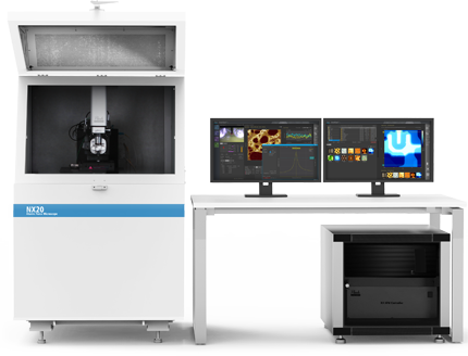
大样品的缺陷检测成像与分析
Park NX20拥有业界便捷的设计和自动界面,让你在使用时无需花费大量的时间和精力,也不用为此而时时不停的指导初学者。借助这一系列特点,您可以更加专注于解决更为重大的问题,并为客户提供及时且富有洞察力的失效分析报告。
-
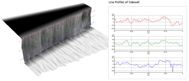
样品侧壁三维结构测量
NX20的创新架构让您可以检测样品的侧壁和表面,并测量它们的角度。众多的功能和用途正是您的创新性研究和敏锐洞察力所必需的。
-
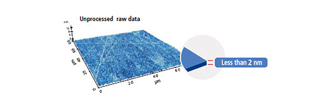
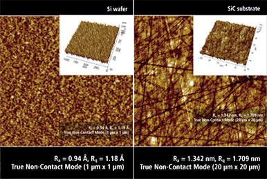
对样品和基片进行表面光洁度测量
表面光洁度测量是Park NX20的关键应用之一,能够带来精准的失效分析和质量保证。
-
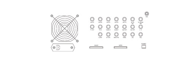
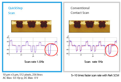
高分辨率电子扫描模式
QuickStep SCM: 快捷的扫描式电容显微镜 PinPoint AFM: 无摩擦导电原子力显微镜
-
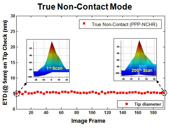
多种创新的前沿技术帮助顾客减少测试时间
通过对比重复扫描情况下探针针尖的形状变化,您可以轻易看到Park的真正非接触模式的优势所在。 借助真正非接触模式,探针针尖在扫描氮化铬样品(即探针检测样品)200次后仍可保持锋利的状态。氮化铬的表面粗糙且研磨性强,会让普通的探针很快变钝。
-
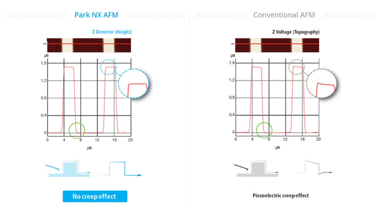
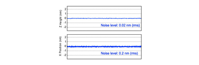
没有压电蠕变误差的真正样品表面形貌
低噪声Z探测器,噪音水平低于0.02 nm,从而达到非常精准样品形貌成像,没有边沿过冲无需校准。Park NX20在为您提供好的数据的同时也为您节省了宝贵的时间。